TO
1 - 25 of 5
| Creator | Title | Description | Subject | Date | ||
|---|---|---|---|---|---|---|
| 1 |
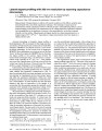 | Williams, Clayton C. | Lateral dopant profiling with 200 nm resolution by scanning capacitance microscopy | Measurement of dopant density in silicon with lateral resolution on the 200 nm scale has been demonstrated with a near-field capacitance technique. The technique is based upon the measurement of local capacitance between a 100 nm tip and a semiconducting surface. Lateral dopant imaging is achieved b... | Dopant profile; Doping density; Scanning capacitance microscopy | 1989 |
| 2 |
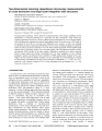 | Williams, Clayton C. | Two-dimensional scanning capacitance microscopy measurements of cross-sectioned very large scale integration test structures | Scanning probe technology, with its inherent two-dimensionality, offers unique capabilities for the measurement of electrical properties on a nanoscale. We have developed a setup which uses scanning capacitance microscopy (SCM) to obtain electrical information of cross-sectioned samples while simul... | Oxide capacitance; Dopant profile; Scanning capacitance microscopy | 1996-01 |
| 3 |
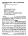 | Williams, Clayton C. | Direct imaging of SiO2 thickness variation on Si using modified atomic force microscope | Fabrication techniques of metal-oxide-semiconductor ~(MOS) transistors have been improved very rapidly during the last several decades. With this trend, scaling down of MOS transistors is necessary to improve the speed of circuits and the packing density of discrete devices. Both lateral and vertic... | Silicon dioxide; Oxide layer; Phosphorus ions; Oxide capacitance; Dopant profile | 1996-03-01 |
| 4 |
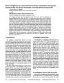 | Williams, Clayton C.; Huang, Yufeng | Direct comparison of cross-sectional scanning capacitance microscope dopant profile and vertical secondary ion-mass spectroscopy profile | The scanning capacitance microscope (SCM) has been shown to be useful for quantitative 2D dopant profiling near the surface of silicon. An atomic force microscope is used to position a nanometer scale tip at a silicon surface, and local capacitance change is measured as a function of sample bias. A ... | Oxide capacitance; Dopant profile; Oxide layer; Scanning capacitance microscopy | 1996-01 |
| 5 |
 | Williams, Clayton C.; Huang, Yufeng | Quantitative two-dimensional dopant profile measurement and inverse modeling by scanning capacitance microscopy | Quantitative dopant profile measurements are performed on a nanometer scale by scanning capacitance microscopy (SCM). An atomic force microscope is used to position a nanometer scale tip at a semiconductor surface, and local capacitance change is measured as a function of sample bias. A new feedback... | Dopant profile; Capacitance change; Scanning capacitance microscopy; Feedback control | 1995 |
1 - 25 of 5